
Author: Ida

Modular PVD cluster systems: Building with the Flextura platform

Celebrating 10 years anniversary for the Flextura PVD platform, we summarize the most important development steps for this platform.

Development Step: Modularity
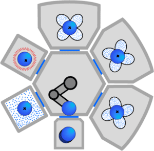
Flextura PVD configuration

From the very beginning, one idea has been at the heart of the Flextura® PVD platform: the system should be able to grow with future needs.

Every Flextura process module, whether a sputtering module, an evaporation module, a GLAD module, or an etch and degas station, is designed to work in multiple configurations.

  1. Start with a single substrate load lock for focused, standalone research.
  2. Step up to cassette loading when throughput demands increase.
  3. Connect the same module to a fully automated cassette-to-cassette cluster when your facility is ready for volume production or your product needs multiple process steps without vacuum breaks.

The module itself is the same. Only the system around it grows.

As Christian Kjelde, Sales Manager at Polyteknik, reflects; “designing the Flextura PVD platform from scratch, meant modularity could be made a core priority. One of the greatest long-term benefits for customers”.

Scale up, without starting over

A researcher might begin with a single Flextura Sputter module and a load lock – a compact, high-quality tool that fits in a small cleanroom and delivers serious thin film results from day one.

Years later, as the development matures and production demands follow, that same core module can be plugged directly onto a Flextura Cluster platform, joined by an evaporation module, a high-temperature deposition chamber (up to 1000°C), or in-system analytical module – all without discarding the original investment.

The Flextura 200 Cluster illustrates this thinking at its most complete. A 200mm platform that is truly almost plug-and-play, allowing process modules to be added as the need for capacity or new processes increases. A proven Brooks MAG LEAP robot handles wafer transport between modules, while the platform accommodates everything from standard SEMI cassettes to custom carriers for even greater flexibility.

For research environments, the Flextura R&D Cluster takes the concept further still. It unveils a new way of modular thinking for PVD systems. From a single chamber with evaporation or sputtering as a standalone system, to an efficient research and development cluster tool with multiple advanced processes. Analytical modules can be attached to the cluster, enabling in-situ characterisation without ever breaking vacuum.

All process modules can be integrated into the Flextura Cluster platform or delivered as standalone tools, with single-substrate, cassette, or batch load-lock configurations.

The Flextura way of thinking lets capital investment follow the increasing demands of a facility.
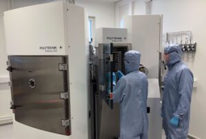
SINTEF Industry & Polyteknik

A decade of thin‑film research built on the Flextura PVD platform — designed to grow. 
Flextura PVD system at SINTED Industry
SINTEF is one of Europe’s largest independent research organisations, with more than 2,200 employees representing over 80 nationalities. At SINTEF’s thin‑film laboratory in Oslo, functional material coatings are developed for applications including gas separation membranes, sensors, batteries, solar cells, and electrolysis cells.

The customer brief: Purpose-built to grow with our research

Ten years ago, SINTEF Industry approached Polyteknik with a clear and concrete challenge: to develop a PVD system tailored for advanced thin‑film research, one that could accommodate a wide range of materials and provide the freedom to explore new material combinations as ideas evolved.

“We needed a system with a high level of flexibility, where we could explore deposition of a wide range of materials and material combinations. It was essential that the equipment did not limit the research, but rather enabled it.”
— Marit Stange, Senior Research Scientist, SINTEF Industry

The Flextura Platform, Modular by design

The Flextura PVD platform was developed to meet the requirements from SINTEF and introduced a new way of thinking: modular, scalable, and designed to grow with the researcher’s ambitions. Start with a single process module, add chambers and analytical tools as needs evolve.  Automated deposition and analysis reduce time spent on routine operation – leaving more time for data interpretation, insight generation, and discovery of the next promising material.

Enabling SINTEF’s Thin‑Film Deposition Platform

The Flextura delivers high-quality, high-uniformity layers of metals and oxides on wafers, with multiple RF and DC magnetron sources in planar or confocal configurations. The system supports deposition ranging from relatively simple metals and alloys to reactive sputtering of oxides and nitrides. High‑temperature deposition up to 800 °C and residual gas analysis (RGA) provide the necessary level of process control.

In addition, an electron beam evaporation chamber dedicated for deposition of silicon for solar cells and battery applications allows growth of silicon at temperatures between RT and 1000 °C.

A partnership built on mutual ambition

Both SINTEF and Polyteknik share the same belief: the best equipment is created in close dialogue with the people who use it. As Flextura marks its 10th anniversary in 2026, SINTEF stands as proof that a platform designed to grow has given the best options for development.

Research that makes a difference

SINTEF Industry was Polyteknik’s first Flextura customer, and today systems are installed at R&D and industrial facilities across Europe.


10 Years of Flextura · Anniversary Series
Issue 01 · 2026

Chip innovation taking root in North Jutland

Aalborg University has just announced the production of a unique gallium oxide power chip, developed at a fraction of the cost of current market alternatives and with the ambition of bringing industrial-scale chip production to North Jutland.

As a supporter of this initiative, Polyteknik share the ambition of bringing industrial-scale chip production to North Jutland. At Polyteknik, we believe that a dedicated cluster of chip-related companies, in North Jutland and across Denmark, is not just a possibility, but a strategic priority.

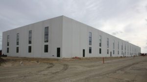
We are working continuously to play our part in making that vision a reality. Construction of our new headquarters and PVD facility in Hjallerup continues to progress, and we are proud to see it take shape.

The facility featuring a 700 m² cleanroom, 3,510 m² of production space, and 2,250 m² of offices, will unite engineering, development, and manufacturing under one roof, significantly expanding our capacity to deliver advanced wafer-based PVD systems to the semiconductor industry and research institutions across Europe.

Read the PR from Aalborg University: Aalborg University has produced a unique power chip – Aalborg University

New PVD facility in Hjallerup advance according to plan

Construction of our new headquarters and PVD facility in Hjallerup is progressing according to plan, marking an important milestone in our continued growth. As announced last summer with the groundbreaking of the new facility, the project represents a significant investment in expanding our capabilities within physical vapor deposition (PVD) technologies and advanced thin-film solutions.

As semiconductor technologies become increasingly critical for industries ranging from AI and advanced computing to automotive, energy and space, the need for specialized materials processing and deposition technologies continues to grow.

Our expansion comes at a time when Europe is placing renewed strategic focus on semiconductor technologies. With the adoption of the European Chips Act, the European Union aims to strengthen the European semiconductor ecosystem and double its share of global chip production to 20 percent by 2030. The initiative mobilizes billions of euros in investment across research, innovation and manufacturing to secure resilient supply chains and technological advancement.

Jens William Larsen, CEO of Polyteknik:

“This new facility represents an important step in Polyteknik’s growth. By expanding our engineering and PVD capabilities, we are strengthening our ability to support customers developing the advanced technologies that will shape the future of Europe’s semiconductor industry”

The expanded headquarters will bring together engineering, development and production capabilities in one modern location. The new facility will include a 2,250 m² office building and 3,510 m² of production facilities, including a 700 m² cleanroom. With a new cleanroom and significantly increased floor space, the facility will support future innovation and growth for both the local community and us.

Once completed, the facility is expected to multiply Polyteknik’s capacity and create new opportunities for developing and manufacturing advanced PVD systems for advanced thin film research and production.

Construction of the new facility is progressing according to plan, and we look forward to sharing further updates as the project moves toward completion.

Polyteknik HQ

Meet us at these events in 2026

We will be present at quite a few events in 2026, and we hope to meet you there!

You are always welcome to contact us at sales@polyteknik.dk, or one of our first points of contact, if you want to book a meeting or you have other inquiries.
We are looking forward to seeing you in 2026!


Webbureau ITTP

Cookie Policy

What is a cookie?

A cookie is a small datafile that is saved on your computer, tablet or mobile phone. A cookie is not a program that can contain harmful programs or viruses.

How/why the homepage uses cookies

Cookies are necessary for the homepage to function. Cookies help us get an overview of your visit to the homepage so that we can continually optimise and adjust the homepage to your requirements and interests. For example, cookies remember what you might have added to a shopping cart, if you have previously visited the page, if you are logged in and what languages and currency you want displayed on the homepage. We also use cookies to target our ads to you on other homepages. On a very general level, cookies are used as part of our services in order to show content that is as relevant as possible to you.

How long are cookies saved?

How long cookies are saved on your device can vary. The time when they are scheduled to expire is calculated from the last date you visited the homepage. When cookies expire, they are automatically deleted. You can view a complete list of cookies below.

This is how you can reject or delete your cookies

You can always reject cookies on your computer, tablet or phone by changing your browser settings. Where these settings can be found depends on the type of browser you are using. If you do change the settings, please be aware that there will be some functions and services that you cannot use because they rely on the homepage being able to remember the choices you have made.

You can choose to not receive cookies from Google Analytics here.

Deleting cookies

You can delete cookies that you have previously accepted. If you are using a PC with a recent version of a browser, you can delete your cookies by using these shortcut keys: CTRL + SHIFT + Delete.

If the shortcut keys do not work and/or you are using an Apple computer, you must find out what browser you are using and then click on the relevant link:

Remember: If you are using several different browsers, you must delete the cookies in all of them.